Materials
Carbon nanotubes
A carbon nanotube is a cylinder of carbon atoms, closed or open at the ends, only a nanometre or so across and often thousands of times longer than it is wide. For two decades it was one of the most studied objects in materials science, and it remains a standard example of how shape at the nanoscale decides properties.
Structure: a rolled sheet
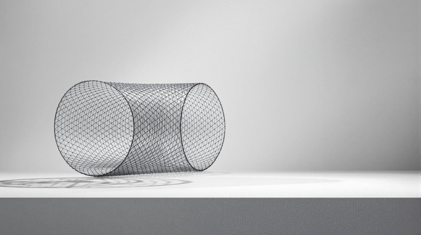
The simplest way to picture a nanotube is to start with graphene, a flat sheet of carbon atoms arranged in hexagons, and roll it into a seamless tube. The Wikipedia article on carbon nanotubes describes the two broad classes this produces. Single-walled nanotubes, idealised as a graphene sheet rolled into a hollow cylinder, have diameters of around 0.5 to 2.0 nanometres. Multi-walled nanotubes consist of several such tubes nested one inside another, like the rings of a tree seen end on; double- and triple-walled tubes are special cases.
The way the sheet is rolled matters enormously. Rolling along one direction lines the hexagons up in a pattern called armchair; rolling along another gives zigzag; anything in between produces a helical, or chiral, tube. The same article notes that some single-walled structures conduct electricity well while others are semiconductors. Which one a given tube turns out to be depends, in the standard theoretical picture, on exactly how its sheet is rolled. A material whose electronic character depends on a twist of a few degrees was bound to fascinate physicists, and it posed an equally large practical problem: most methods of making nanotubes produce a mixture.
A contested discovery
Ask who discovered carbon nanotubes and the answer depends on whom you ask. The Wikipedia article is frank that the identity of the discoverers is controversial. Much of the academic and popular literature credits Sumio Iijima of NEC with a 1991 paper on hollow, nanometre-sized tubes of graphitic carbon, and that paper set off the modern research field. But the article also discusses earlier reports of tubular carbon structures and cites a 2006 editorial in the journal Carbon that reviewed the question. The article adds that in 1993, groups led by Iijima and Ichihashi at NEC and by Bethune and colleagues at IBM independently found that adding transition metals such as iron and cobalt to vaporised carbon catalysed the formation of single-walled tubes, which opened the way to producing them deliberately.
That sequence explains the shape of the literature. Papers from the early 1990s are dominated by multi-walled tubes and by debates about structure; from the mid-1990s single-walled tubes take over, with a growing emphasis on synthesis, purification and measurement of individual tubes.
Properties
According to the same article, nanotubes combine exceptional tensile strength and thermal conductivity, both consequences of their structure and of the strength of the carbon–carbon bond, and they can be chemically modified. Those properties made them candidates for composite materials, electronics, optics and sensors. In practice, turning the properties of an individual tube into the properties of a bulk material proved much harder than early papers hoped: tubes bundle together, vary in length and type, and are difficult to align or to bond to a surrounding matrix. A large share of the literature is about exactly those practical problems.
Nanotube transistors
The electronic potential of semiconducting tubes led directly to the nanotube field-effect transistor, in which a single tube or an array of tubes replaces the silicon channel of a conventional transistor. The Wikipedia article on carbon nanotube field-effect transistors records that such devices were first demonstrated in 1998 and that there have been major developments since. The motivation, as that article explains, is the long-running effort to keep shrinking transistors as conventional silicon approaches its limits.
For readers of the literature from around 2001 and 2002, nanotube electronics is one of the most visible themes: papers on metal contacts to tubes, on turning p-type devices into n-type ones, on combining several tube transistors into simple logic, and on separating metallic tubes from semiconducting ones. The page on 2001–2002 places that work in its wider setting, and molecular electronics and nanowires covers the neighbouring subjects.
Relatives and successors
Nanotubes belong to a family of carbon structures that also includes the closed cages known as fullerenes and the flat sheet of graphene. Historically the order of attention ran cage, tube, sheet: fullerenes in the late 1980s, nanotubes in the 1990s, graphene after 2004. Much of the vocabulary, and many of the measurement techniques, passed from one to the next, so a reader who understands one of the three has a head start on the others.
Nanotubes have also appeared in less expected places. The history of nanotechnology article reports that carbon nanotubes have been found in ancient pottery from Keeladi in India, though it is not known how they formed or whether they were made deliberately. Carbon, it seems, has been curling itself into tubes for far longer than anyone has been looking.