Materials
Graphene and atom-thin carbon
Graphene is the simplest of the carbon nanostructures and, for a long time, the one most people thought could not exist on its own. It is a single layer of carbon atoms joined in hexagons, the flat sheet from which a nanotube can be imagined as rolled and from which graphite is stacked.
A honeycomb one atom thick
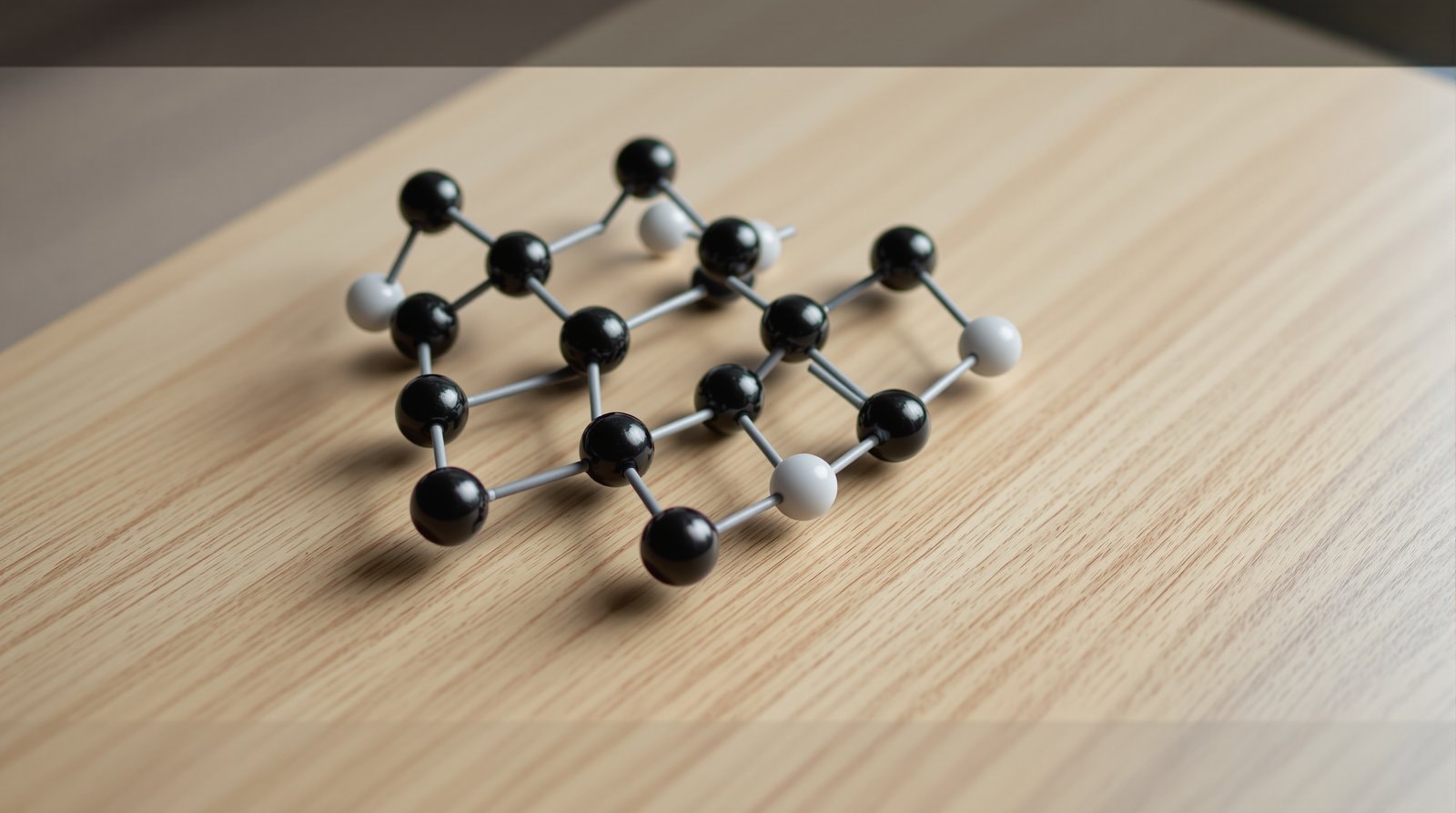
The Wikipedia article on graphene describes it as a carbon allotrope consisting of a single layer of atoms arranged in a honeycomb planar nanostructure. When many hundreds of layers stack up, the result is graphite. The name joins graphite to the suffix -ene, which chemists use to signal double bonds. The article lists the properties that made the material famous: exceptionally high tensile strength, high electrical conductivity, transparency, and the distinction of being the thinnest two-dimensional material known. It adds, with some care, that on a microscopic scale graphene is the strongest material ever measured.
Theory long before the sheet
Graphene was a theoretical object for decades. The same article records that its existence was first theorised in 1947 by Philip R. Wallace, during his research on the electronic properties of graphite, and that the word graphene was first defined in 1987 by Hanns-Peter Boehm, who with co-workers had isolated single sheets from graphite. For most of the second half of the twentieth century, however, many physicists doubted that a truly two-dimensional crystal could be stable in isolation. That doubt is part of why the 2004 result drew so much attention.
Pencil, paper and sticky tape
The Nobel Prize popular information for the 2010 physics prize tells the isolation story in plain terms. Graphite is made of layers weakly held together, which is why a pencil leaves a trace; the prize text notes that one millimetre of graphite consists of three million layers of graphene. Andre Geim and Konstantin Novoselov at the University of Manchester used adhesive tape to peel thin flakes from a piece of graphite, repeating the process ten to twenty times until the flakes became very thin. Their second insight was how to find the rare single layers among the thicker debris: they placed the flakes on a plate of oxidised silicon, where interference colours in an ordinary optical microscope reveal how many layers a flake contains.
The method was almost comically simple, and its simplicity mattered. It meant that any laboratory with graphite, tape, silicon wafers and a microscope could begin work on graphene, which is one reason the literature grew so quickly after 2004.
The 2004 paper
The research report itself appeared in Science in October 2004. In it, Novoselov and colleagues described monocrystalline graphitic films a few atoms thick that were nonetheless stable under ambient conditions, metallic, and of remarkably high quality. Their abstract reports that the films behave as a two-dimensional semimetal with a tiny overlap between the valence and conduction bands, and that they show a strong ambipolar electric field effect: applying a gate voltage could induce either electrons or holes in the film at high concentration and with high mobility at room temperature.
The phrase "electric field effect" is the key to why physicists cared. A field effect is what a transistor uses: a voltage on a nearby gate changes how many charge carriers a channel contains. Showing that a film a few atoms thick could be switched in this way, with carriers that moved easily at room temperature, suggested both new physics and a possible route to new electronics. The prize text describes how the 2004 article stirred up a great deal of attention worldwide for exactly those two reasons.
The 2010 Nobel Prize
Six years after the Science paper, Geim and Novoselov received the Nobel Prize in Physics. The Wikipedia article gives the committee's wording, which recognised their groundbreaking experiments regarding the two-dimensional material graphene. The short interval between discovery and prize is unusual in physics and reflects how quickly the result was confirmed and extended by other groups.
What followed
Graphene opened a door rather than closing one. Once it was clear that a stable crystal one atom thick could be isolated, researchers went looking for others, and the idea of two-dimensional materials became a field of its own. Within graphene research, much of the later literature concerns problems the early papers left open: how to make large sheets rather than small flakes, how to open an energy gap so that graphene transistors can be switched fully off, and how to combine graphene with other thin layers. The Wikipedia article notes that attempts to scale and automate production have had limited success so far, because of concerns about cost and quality control.
For readers following the literature, graphene is also a good lesson in how a subject moves between journals. Its first report was in a general-science weekly; its physics soon filled Physical Review Letters and Physical Review B; its chemistry and device work spread through the materials and nanoscience titles. The neighbouring carbon forms are described on the carbon nanotubes and fullerenes pages, and the way single-layer flakes are imaged is discussed under probe microscopy.