Tools and devices
Seeing and touching atoms: STM and AFM
Before 1981, individual atoms on a surface could be inferred but not routinely seen. The scanning tunnelling microscope changed that, and within a few years a family of related instruments let researchers image, measure and even move single atoms. Much of what nanoscience knows about surfaces was learned with a sharp tip and a very steady hand.
A tip, a surface and a feedback loop
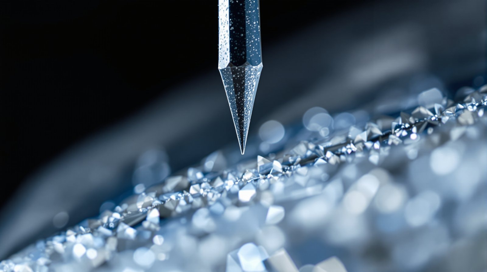
Every scanning probe microscope works on the same basic plan. A very sharp tip is brought extremely close to a surface and moved across it in a raster, line by line, while some interaction between tip and surface is measured at each point. The Wikipedia article on scanning probe microscopy explains that the field was founded in 1981 with the invention of the scanning tunnelling microscope, that the key to Gerd Binnig and Heinrich Rohrer's success was a feedback loop regulating the gap between tip and sample, and that piezoelectric actuators make it possible to position the tip with atomic precision. The result is a grid of numbers, usually shown as a false-colour image.
The scanning tunnelling microscope
The first of these instruments relied on a quantum effect. The Wikipedia article on the scanning tunnelling microscope explains that when a conducting tip is brought very near a conducting surface and a small voltage is applied, electrons can tunnel across the vacuum gap between them. The tunnelling current depends very steeply on the distance, so tiny changes in height produce large changes in current. The article states that the instrument can distinguish features smaller than 0.1 nm laterally with 0.01 nm depth resolution, which means individual atoms can routinely be imaged and manipulated. Most instruments work in ultra-high vacuum at very low temperature, but versions exist for air, water and high temperatures.
The same current carries more than height. By holding the tip still and sweeping the voltage, a technique called scanning tunnelling spectroscopy measures the local electronic structure of the surface under the tip, which is how many papers on nanotubes, molecules and quantum dots probe the energy levels of a single object rather than an average over many.
The press release for the 1986 Nobel Prize in Physics announced that half the prize went to Binnig and Rohrer of IBM's Zurich research laboratory for their design of the scanning tunnelling microscope, and the other half to Ernst Ruska for his work on electron optics and the first electron microscope. The release makes a nice point about terms: the tunnelling instrument is not a true microscope in the sense of forming a direct image, since it builds its picture from a measured interaction point by point.
The atomic force microscope
Tunnelling requires a conducting sample, which rules out most insulators and much of biology. The atomic force microscope removes that limit by measuring force instead of current. According to the Wikipedia article on atomic force microscopy, a sharp tip on the end of a small cantilever is scanned over the sample; forces between tip and surface bend the cantilever, and the bending is detected by a laser beam reflected from its back onto a photodiode. The instrument then adjusts the cantilever's height to keep the signal constant, and the height record traces the surface.
The article records that the first publication on the technique, by Binnig, Quate and Gerber in 1986, speculated about atomic resolution, but that achieving it took years of further work. Because it works on insulators and in liquids, the atomic force microscope became the workhorse of nanoscience: it measures the height of graphene flakes, the diameter of nanotubes, the shape of self-assembled films and the structure of biological molecules on surfaces.
A growing family
Once the basic idea was established, researchers attached almost every measurable interaction to a scanning tip. The scanning probe microscopy article lists dozens of variants, including magnetic force microscopy, which maps magnetic domains; Kelvin probe force microscopy, which maps surface potential; conductive atomic force microscopy, which measures current through the tip; and piezoresponse force microscopy. The same tip can also be used to write: dragging it, heating it or applying voltage lets researchers pattern surfaces at the nanoscale, a subject taken up on the nanofabrication page.
Reading a probe image
Probe images are persuasive, and a careful reader should treat them with the same care as any other measurement. The colours are a choice made by the software, not a property of the sample. The apparent shape of small objects is broadened by the finite size of the tip, so a nanotube can look wider than it is while its height is reliable. Artefacts from a double tip, drift during a slow scan, or contamination picked up by the tip can all produce convincing-looking features. Good papers show scale bars, state scan conditions, and back important claims with images of more than one area or with a second technique.
Scanning probes and electron microscopes are complementary, and many papers use both. For the electron side, see electron microscopy at the nanoscale; for the history that made these instruments central to the field, see where the idea came from.